NCEPB303GU
General Features
Q1 “High Side” MOSFET:
- VDS =30V,ID =30A RDS(ON) <5.8mΩ @ VGS=10V RDS(ON)<8.9mΩ @ VGS=4.5V
Q2 “Low Side” MOSFET:
- VDS =30V,ID =100A RDS(ON) <1.9mΩ @ VGS=10V RDS(ON) <2.8mΩ @ VGS=4.5V
- Excellent gate charge x RDS(on) product(FOM)
- Very low on-resistance RDS(on)
- 150 °C operating temperature
- Pb free terminal plating
- RoHS compliant
- Halogen free
Application
- Compact DC/DC converter applications
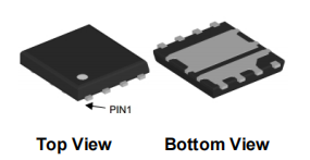
The NCEPB303GU uses Super Trench technology that is uniquely optimized to provide the most efficient high frequency switching performance. Both conduction and switching power losses are minimized due to an extremely low combination of RDS(ON) and Qg. It includes two specialized MOSFETs in a dual Power DFN5x6 package.
Products
Related Topics
[contact-form-7 id="6bab151" title="Contact form"]
Login
Register
