NCEB301G
Q1 “High Side” MOSFET
- VDS= 30 V,ID= 20 A RDS(ON)< 7.2 mΩ @VGS=10V (typical: 6.1 mΩ) RDS(ON)< 12.5 mΩ @VGS=4.5V (typical: 9.6 mΩ)
Q2 “Low Side” MOSFET
- VDS= 30 V,ID= 35 A RDS(ON)< 4.1 mΩ @VGS=10V (typical: 3.5 mΩ) RDS(ON)< 7.8 mΩ @VGS=4.5V (typical: 5.9 mΩ)
- Excellent gate charge x RDS(on)(FOM)
- Very low on-resistance RDS(on)
- 150°C operating temperature
- Pb-free lead plating
- 100% UIS tested
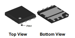
The NCEB301G is designed to provide a high efficiency synchronous buck power stage with optimal layout and board space utilization. It includes two specialized MOSFETs in a dual Power DFN5x6 package. The Q1 "High Side" MOSFET is designed to minimize switching losses. The Q2 "Low Side" MOSFET uses advanced trench technology and design to provide excellent RDS(ON) with low gate charge.
Products
Related Topics
[contact-form-7 id="6bab151" title="Contact form"]
Login
Register
